My wife goes to bed long before me, so when I go to bed, it behooves me to do so without significant light or racket. After countless nights of fiddling with a 3-sided micro-USB cable in the dark, I bought this neat little USB phone charger. It’s not the cheapest, nor the priciest, but was approximately the size and shape of my phone (less risk of our cat bumping it off a tiny pad during the night and waking us up), and lives up to its promise of cool operation, especially while not charging (meaning it is not constantly guzzling power trying to charge a device that isn’t there).
But…
This charger also came with one untenable drawback: this gadget for charging my phone without any noisy fiddling about, comes with a built-in noisemaker that beeps loudly every time you put a device on it to charge. That’s bad enough for a one-time event, but if the phone is placed or later bumped off-center (i.e. the cat’s been anywhere near the nightstand), it will go on beeping all through the night as the charger detects the phone intermittently. So if the ladies don’t find you handsome…
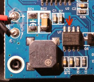
First off, the part you’re probably here for: how to silence that infernal beeping sound once and for all, without soldering. Open the charger (there are 4 small screws hidden beneath the rubber feet), find the 8-pin chip in the lower-left and use your favorite small tool (nippers, X-Acto, etc.) to cut the indicated pin. This pin directly drives the piezo buzzer (tall square part in the bottom-left corner). Of course, you can also cut, desolder or otherwise neutralize either of these parts in its entirety too if you have the time and a soldering iron, but I think cutting the one pin is easier.

While we’re in here, let’s have a look at the circuitry. There’s actually rather a lot of it – I was expecting a massively integrated single-chip solution, but there’s a surprising pile of discretes in here, including a total of 12 opamps.


The main IC, U5 in the center, is an “ASIC for QI Wireless Charger” manufactured by GeneralPlus. At the time of this writing, their site is rather less than forthcoming with specs or datasheets. This is driving a set of 4 MOSFETs (Q1 ~ Q4) via a pair of TI TPS28225 FET drivers (U1, U4) to drive the ludicrously thick charging coil. The coil itself is mounted to a large ferrite disk resembling a fender washer, which in turn is adhered to a piece of adhesive-backed foam – probably to dampen any audible vibrations as the coil moves in response to nearby magnetic or ferrous objects as it is driven (such as components in the device being charged). The parallel stack of large ceramic caps (C12, C14, C15, C18), along with the coil thickness itself, gives a hint as to the kinds of peak currents being blasted through it.
For fans of Nikola Tesla, this planar coil arrangement should look oddly familiar. Qi inductive charging, like most contemporary twists / rehashes / repatentings of this idea, extend it by using modern cheap-as-chips microcontrollers to allow the charger and chargee to talk amongst themselves. This allows them to collude to tune their antennas for maximimum transfer efficiency, negotiate charging rate, perform authentication (maybe you don’t want freeloaders powering up near your charger) or etc. In the case of Qi, the communication is unidirectional – chargee to charger – and used to signal the charger to increase or decrease its transmit power as needed. This provides effective voltage regulation at the receiving end and can instruct the charger to more-or-less shut down when charging is complete. Communication is achieved via backscatter modulation, similar to an RFID tag.
The chips to the left and right of the Qi ASIC, U2 and U3, are LM324 quad opamps. Without formally reverse-engineering the circuit, my gut says these opamps circuits, surrounded with RC discretes like groupies at a One Direction concert, are likely active filters, probably involved in sensing the backscatter modulated signal and overall power impact of the chargee, if any. Again, this is just educated guessing without actually tracing out the circuitry (which would involve more time than I care to spend).
The chip at the bottom right, U6, is an LM358 dual opamp, with what is probably a LM431-compatible voltage reference (U8) a bit to its left, acting directly as a 2.5V reference (cathode and reference pin tied together). At least one pin of the LM358 is visibly supplying the power to the charge-indicator LED, so it’s a reasonable guess this circuit is there to control both LEDs in response to the voltage loading produced by a device during charge. Finally, U7 near the bottom-left, noted earlier as driving that irritating-ass beepy speaker, is a 555 timer that provides the actual oscillation to drive the charge-indication beep in response to a momentary signal from elsewhere (it disappears underneath the ASIC). Q5 is most likely acting as a power switch for U7, keeping it disabled (unpowered) between beeps.
One final note completely unrelated to any teardown of the device itself: it comes with a troll USB cable. That is to say, while it looks like a regular USB cable, and may easily get mixed in with the rest of your stash, it’s actually missing the data wires entirely and only provides power. While this is not unreasonable considering it’s just a charger, beware not to let this cable get mixed in with ‘real’ ones unless you’re pulling a prank on someone. Otherwise it’ll come back to bite you some months later when you grab the nearest cable, plug it into a gadget and it’s mysteriously stopped working.
Leave a Reply