I recently assembled a set of prototype boards for a particular project at my day job, and ran a math- and memory-intensive test loop to test them out. Two of the boards ran the code fine, but one crashed consistently in a bizarre way that suggested corruption or otherwise unreliability of the RAM contents.
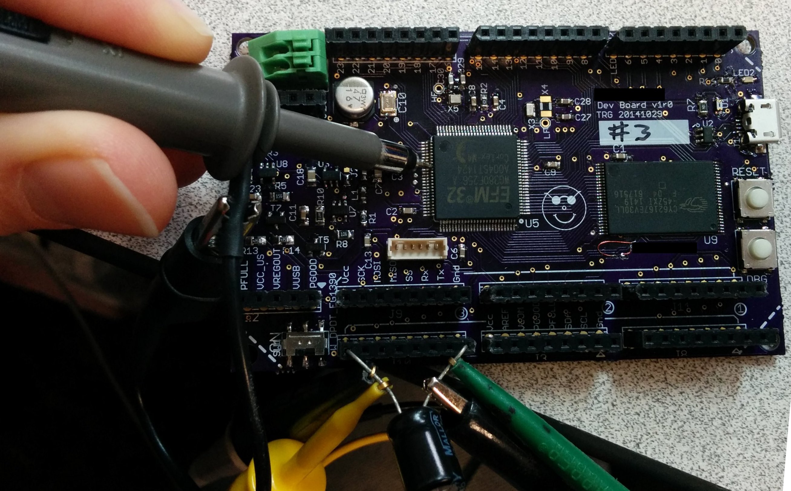
Since the other two identical boards worked, a hardware/assembly defect was the likely explanation. These boards feature a 100-pin TQFP CPU and 48-pin SRAM with 0.5mm lead pitch, all hand-soldered of course, but a good visual inspection turned up no obvious defects.
The first thing I tried was a quick-n-dirty RAM test loop that wrote the entire RAM with an address-specific known value and immediately read it back (in this case, it was just the 32-bit RAM address itself), but this (overly simplistic, it turns out) check didn’t report any failures. However, I did notice the current reading on my bench supply occasionally spiking from 0.01A to 0.04A. This board uses a low-power ARM micro specifically chosen for efficiency, and should rarely draw more than about 15mA at full tilt, so this was a red flag.
With this in mind, the next thing I did was get a higher-resolution look at what was going on with the current. The CPU vendor provides a sweet energy profiling tool for use with its pre-baked development kits, which also double as programmer and debugger for the kit and external boards. The feature works by sampling input current to the development kit via a sense resistor at high speed, and optionally coupling it to the running program’s instruction counter via the debugger to estimate energy usage for each function in your program. By uploading a dummy program to the kit that just puts it into a deep sleep, and tying the external board into its VMCU/GND pins, it can be used with any external target board that draws up to 50mA or so.
Running the memory test again with the profiler active, I got the following:
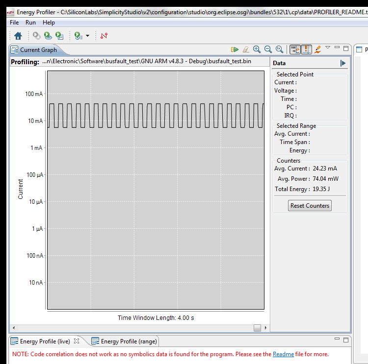
Again, the kit can supply a max of 50mA or so, and this graph shows a repeating cycle which spends half the time somewhere a bit northward of this. Sure enough, probing the supply voltage with a scope, the voltage drops a bit whenever the overcurrent occurs. A memory test loop should draw a fairly constant current; it shouldn’t vary with time or data or address as this appears to be doing. So it’s a safe bet that one of the address or data pins to the external RAM is shorted. But where?
I could begin probing address and data lines to find the ones that toggled at the same rate as the dip on the voltage rail, but on a wild hare (or hair) picked up our new secret weapon (not the Handyman’s Secret Weapon), an IR thermal camera.
Just after power-on with the RAM test running, I saw this:
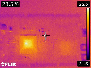
The part immediately to the left of the crosshair is the CPU. It wasn’t detectably warm to the touch, but here it’s easy enough to see where the die itself sits inside the chip package. There is also an apparent ‘hotspot’ roughly centered along the lefthand edge of the die. The I/O pins just next to this hotspot are address lines tied to the RAM. While it isn’t *always* the case due to the vagaries of chip layout, the GPIO pin drivers are almost always situated at the edges of the die, right next to the pins they drive. This is about as close to a smoking gun as you can get without the actual smoke. While it’s hard to see exactly which pin or pins this hotspot corresponds to, it does narrow the search quite a bit! For reference, here is how it looks unpowered.

Scoping a handful of adjacent pins, the issue becomes clear.

Two adjacent address lines to the memory, immediately next to the hotspot, show this decidedly non-quite-digital-looking waveform on them (bottom trace), lining up pretty well with the voltage droop (top trace). This points to not one shorted pin (to GND or etc.), but two adjacent pins shorted together, their on-chip drivers fighting one another to produce these intermediate voltages and consuming excess current in the process. A quick beep-test confirms the short.
It turned out to be a hair-thin solder bridge between two adjacent pins on the SRAM, pictured below. Do you see it?

Yeah, neither did I at first. It was more visible only at a very specific angle…

Note the other apparent “stuff” crossing pins in this angle wasn’t solder, but remnants of a cotton swab used to clean flux from around the pins.
Mapping the I/O drivers and other stuff
Just for fun, I purposely shorted all the GPIOs available on headers to ground and ran a loop that briefly flipped each one high. Here is the result! Note that not all GPIOs on this board were available on a header (many go to the RAM chip), and they are not necessarily pinned out in a logical numeric order. I haven’t specifically tested it yet, but the same method should be usable to unintrusively map out the location of on-chip modules (core/ALU, voltage regulators, AES engines, etc.) that can be exercised individually.
<pipedream>The day when thermal imaging gets good enough we can use IR attacks instead of power analysis to figure out what a chip is doing (encryption keys, etc.) without decapping it…</pipedream>
Leave a Reply