This is the protocol spec and PIC10 firmware download for Das Blinkenlichten (1.2). This version improves handling of the ‘Identify’ command by end devices. Backward compatibility to 1.1 is not affected.
I don’t have pretty datasheets, application notes, timing diagrams, or much example code / pseudocode, but I’m sick of sitting on this thing until I get around to those :-P So I figured I’d just stick it on the internet and see what happens. The rest might be filled in in my future spare time (or by some nice person in the comments)…
Description:
Das Blinkenlichten is an open-source RGB LED lighting system and protocol written for the PIC10F200 microcontroller. A complete node consists of this chip, an RGB LED, three current-limiting resistors and a small capacitor for power-supply smoothing. A single chain can have up to 255 unique nodes (or as many non-unique ones as the wires will carry power/data for, without burning up!). Everything is coordinated by a single master device, which can be any low-cost microcontroller or equivalent with a free I/O pin. The beginnings and goals, etc. of the design are described on this page.
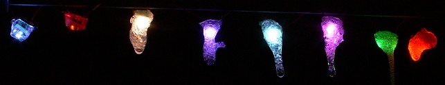
Pretty Pictures
Pic: Blinkenlichten in melty, icicle-like resin
Pic: Swirled around by a girl dancing
Video: Very simple random-color-generator demo
Video: Cool video of blinkenlichten who react to music
Features / Commands in brief:
- Cheap! At 34 cents each (qty:100), the PIC10 is probably one of the world’s cheapest and simplest microcontrollers. Complete parts cost can be less than $1US per node.
- Fast 1-wire data bus – complete operation with only 3 wires (power, data, ground)
- 3 colors (R,G,B) can each be set to one of 9 intensity levels – total 729 possible colors
- Set Group Address command: control groups of LEDs at a time with a single command
- Deferred Update command: Allows simultaneous color changes even with a large number of devices.
- Identify command: Discover the addresses present on the bus.
- Power Save command: Stop all clocks and enter low-power mode until the next command
Arduino/Wiring library and example
Library and example sketch showing common usages (move to /hardware/libraries in your Wiring folder, close and re-open Wiring. The example will then appear under Sketchbook -> Examples -> Library-Blinken). This library is released under the GPL.
Firmware and source code (PIC10 assembler)
Version 1.3 (“It’s Log!” edition) can be donwloaded in this zip file. A few lines at the beginning will have to be set according to your hardware configuration (see below). The “#define MYADDR …” line contains the address the chip should respond to – change this and rebuild for each chip you program. This version adds a logorithmic color table so that the color intensities you specify will appear linear (evenly-spaced steps) to the human eye. Adding this meant some idiotproofing had to be removed – sending an invalid (>8) intensity value will cause undesired operation. Starting with 1.3, this code is released under the GNU General Public License v3.
Version 1.2 (‘dumb’ linear color table) can be donwloaded in this zip file. A few lines at the beginning will have to be set according to your hardware configuration (see below). The “#define MYADDR …” line contains the address the chip should respond to – change this and rebuild for each chip you program.
Hardware/Schematics:
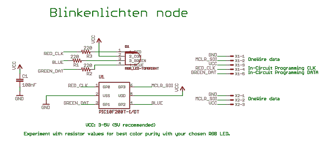
Basic schematic for an individual node. The schematic shown uses a common-anode LED (common is connected to VCC); for a common-cathode, tie the LED common to Ground instead and change the appropriate #define at the beginning of the code. Different LED packages have different pinouts; test and make sure of them before wiring it up – or especially making boards. (The R/G/B connections to the LED can be easily remapped in software, but you have to get the LED’s common right the first time!)
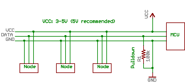
Basic wiring diagram for a complete string with several nodes and a controller. There is a pulldown resistor between the data wire and ground (recommended value 100k ~ 1Meg). This is necessary for the ‘IDentify’ command to work, and it also helps prevent your string of lights from going haywire if the controller takes some time to start up and the voltage on the line is floating.
The maximum cable length, and maximum nodes reliably driven on it (or maximum speed), depends on how strong your controller drives the data line. As you add length and extra loads (inductance and capacitance) to this wire, the voltages on it will take longer to rise and fall, and be more difficult for the nodes to reliably consider a ‘1’ or ‘0’. I’ve run them with 6+m of cable without incident, but if you run into problems, reducing the data rate should help. If you don’t care about the IDentify feature, you can add a beefy buffer here to drive the data line harder. If driving long strings, you might also want to add decent-sized electrolytic capacitors between the power and ground wires at intervals along the string.
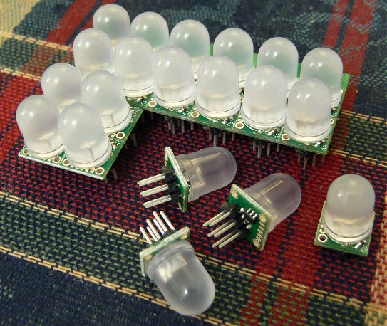
PCB and Parts List (Bill Of Materials)
This file contains a parts list for both DIP/breadboard and tiny surface-mount versions. Also included is an EAGLE schematic and Gerber files for a miniaturized, wearable board using surface-mount components. These data (schematics, BOM and Gerbers) are released into the public domain.
A picture of the finished SMT boards (panel) is shown below. With a jumbo 10mm RGB LED, the board is almost completely concealed behind the LED and only the sewable connections stick out.
Programming the chips
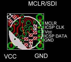
To write the firmware to these chips requires access to a PIC programmer. The official ones made by Microchip Inc. are quite expensive; fortunately there are many clones out there that work just as well, and some open-source designs you can build yourself. Just make sure that the programmer supports the PIC10 devices; some very simple/cheap designs (e.g. direct to PC serial port) may be designed only for “low voltage program” devices and won’t generate the +13V or so necessary to program this chip. The DIP variants can be programmed in or out-of-circuit; for the SMT variants, you will probably need to solder them to your board (with an appropriate pin header / etc for the programming lines), program the chip, and THEN add the LED (since it shares some of the programming pins and will interfere). For the ready-made SMT circuit board above, the following drawing indicates the pinout of the programming header on the edge of the board. For this, I soldered the wires from the programmer to the “wrong” side of a 5-pin 1.25mm connector (such as Molex 53047-05), then just press the other end into the PCB during program.
Command packet format: (forgive the horrible ASCII art)
<start> <addr[7..0]><cmd[7..0]><stop>
_____- - - -. . . 16 data bits . . .______
The bus idles low.
Start condition: Bus goes HIGH and stays high for longer than the longest possible loop run (min. ~ 17uS), so that all devices are guaranteed to catch it.
Data bits consist of a low period (low half) followed by a high period (high half). A 1 is denoted by making the LOW half longer than the HIGH half, and a 0 by making the HIGH half longer. Ideally, all bits should total the same length, but since the low half sets the baud rate on a bit-per-bit basis, this is not required. However, any half should be a minimum 18 device clocks (18/1MHz=18uS) for most accurate timing, and should not exceed 255 device clocks (255uS).
Stop condition: Give some time for the cmd to be processed before sending a new one (bus idles low). If you’re in a hurry, this time depends on the specific cmd. Otherwise, you can just wait about 90uS (time for the longest 1-way cmd, activate_deferred, to complete) and not worry about it. (*See special timing notes for Identify cmd.) This is the preferred approach, but you could also just make the START condition longer.
Address BYTE format:
bit <76543210>
AAAAAAAA
where AAAAAAAA is an 8-bit device address (or group address). Address 0 is the broadcast address. Since the ‘Group Address’ cmd only supports addresses up to 64 (0x40), I recommend a handful of low addresses (0x01 ~ 0x0F) be set asdie for group addresses if you plan to use this feature.
Cmd BYTE format:
bit <76543210>
ERGBIIII
E: Extended Command flag. If ‘1’, decode remaining bits as Extended Cmd as described under Extended Commands. Otherwise,
RGB: Which color(s) cmd applies to (set ‘1’ for each color this intensity applies to)
IIII: Set intensity (0 ~ 8)
Extended Commands
11xxxxxx : Set Group Addr to value xxxxxx
10XXyyyy : Poke "Virtual reg" XX with contents yyyy (see below), where XX is the address of a virtual 4-bit reg and yyyy is the value to poke.
Vreg 00: Flags [x identify activate_deferred power_save]
Vreg 01: Defer buf R
Vreg 02: Defer buf G
Vreg 03: Defer buf B
Detailed description of the virtual registers:
Vreg 01 ~ 03 allow a deferred update to be sent for the R, G and B channel respectively. The new intensity value(s) are stored in memory, but the old intensity values continue to be displayed until an activate_deferred command is executed, at which point the new intensities are displayed. This will be particularly useful for trickling new values over the bus, then sending a single activate_deferred to all devices (addr 0) to give the appearance of a simultaneous update.
Vreg 00 is a virtual register among virtual registers: Rather than writing a value to it, you write to it setting an individual bit to perform the requested action. Once the action is performed, the bit can be considered automatically cleared.
- Unused (bit 3): “No-Op” – Dummy command, doesn’t do anything.
- Identify (bit 2): On receipt of this cmd by a given device address, this device shall pull the data line HIGH (internal weak pull-up) for a period of about 512 device clocks (or whatever, plenty long enough for master device to see it). Normal operation is then resumed. (Note that this may disrupt other devices on the bus, who interpret the pullup signal as a new START command. If this is bothersome an Identify command may be followed immediately by a dummy command if a device responds. The device’s response will be seamlessly eaten by the dummy cmd’s START, so it just looks like an extra-long start bit to all devices.)
- Activate_deferred (bit 1): Replaces the currently displayed intensities with the contents of the Defer (R,G,B) regs if they contain a valid update.
- Power_save (bit 0): This command will effectively stop the CPU and any pulse modulation activities and enter a low-power SLEEP mode. The device will remain in SLEEP mode until the next bus activity occurs, at which point it will re-awaken. Technically it will be waking up occasionally due to WDT, but these activity periods will be brief.
Quick Examples
Set device id 02 Red to max (8):
<start><02><01001000><stop>
Set device id 02 to bright white (Red, Green, and Blue to max):
<start><02><01111000><stop>
Set device id 02 to arbitrary color (Red 8, Green 2, Blue 3):
<start><02><01001000><stop>
<start><02><00100010><stop>
<start><02><00010011><stop>
Set device id 07 off (Red, Green, and Blue to 0):
<start><07><01110000><stop>
Clear all group addresses to 0 (default):
<start><00><11000000><stop>
Assign device id 0x9F to group (address) 05:
<start><9F><11000101><stop>
Set all devices to power save:
<start><00><10000001><stop>
Advanced Examples
Identify all the devices on the bus (pseudocode):
for (id = 1 to 255)
{
Send1Wire(id, b'10000100'); // Extended cmd: Identify
Delay(100); //delay 100 uS, to give device time to respond
DATA_WIRE = 'INPUT'; // However you switch this pin to an input on your preferred platform
gotResponse = DATA_WIRE; // read the data line to check if anyone is responding (pulling the data line high)
DATA_WIRE = 'OUTPUT'; // Switch it back to an output (retaining same value as was read)
if (gotResponse == 1) // Was there a response?
{
print("Found device " , id); // do something with this information, e.g. store active IDs to a table
Send1Wire(0, b'10001000'); // send dummy command if there was a response.
// Or you can just wait a few hundred msec for the other devices to reset
}
}
Specific firmware points of interest
The intensity of the LED colors is controlled using pulse width modulation (PWM). The basic operation is that the intensity value for each color (0 ~ 8) is converted to that many ‘1’s and stored in a register, and this register’s contents are continually rotated in circles. Each time, the last bit is used to determine the on/off state of the LED. So with 8 bits in a register, it can be on 0/8 of the time (off) or 1/8 of the time or … 8/8 of the time (full brightness).
To provide the fastest possible update rate, it’s necessary to squeeze as much performance out of these cheap tiny PICs as possible. The PIC10 supports only a handful of instructions, no interrupts, and only a rudimentary 8-bit timer. For the PIC10F200, the entire program is limited by memory to 255 instructions. Therefore we can’t afford to be too sloppy.
The code uses look-up tables in place of any loops/math wherever possible. The chip does not support table-indexing operations in ROM (Flash), so this is done using computed GOTO: In many microprocessors including this one, the Program Counter register (which acts as the processor’s bookmark in the code’s execution) can be modified by the program directly. Thus, by writing a new value to the Program Counter you can force the processor to lose its place, resuming program execution from the address you just wrote. By performing math operations directly on the program counter, this method can be used to index a lookup table nearby. In the example below, the intensity value is added to the program counter to make it an index into a table stored just after it. The ‘retlw’ instruction returns from the function with a specific value saved in a register. This code snippet converts the (0 ~ 8) value to a value containing that many ‘1’s, using only a few clock cycles.
; Want to return a value containing the number of '1's specified in the intensity
; value. But want to spread them out for faster switching and less perceivable flicker.
setpwm:
movf INDF, w ; cmd value
andlw B'00001111' ; mask off bogus bits
addwf PCL, f ; skip that many instructions
retlw B'00000000' ; 0x00
retlw B'00000001' ; 0x01
retlw B'00010001' ; 0x02
retlw B'01001001' ; 0x03
retlw B'01010101' ; 0x04
retlw B'01010111' ; 0x05
retlw B'01110111' ; 0x06
retlw B'01111111' ; 0x07
retlw B'11111111' ; 0x08 ; last valid value
This same method is used to allow the PWM loops to keep running while receiving data. Each time a bit is received, the PWM loop “jump table” is called. The count of the number of bits received is used as the index into the jump table; instead of a list of data values, each table entry contains a jump (GOTO) to the address of either the red, green or blue updater.
Determining between ‘1’ and ‘0’ bits on the data wire also takes just a few instructions. For each bit, the line is held low for some amount of time by the controller, then held high. Whether the low or high half was longer determines whether it was a 1 or 0. The way to measure this can be thought of as a stopwatch that counts up during the first half, then down during the second half. If the count goes negative, the second half was longer and we record a ‘0’, else we record a ‘1’. The ‘stopwatch’ here is the chip’s 8-bit counter/timer register. But it can’t count down, it can only count up! So a little cheating: when finished timing the first half, we complement (invert) the contents of the timer register. Now it’s still counting up, but if the original count was 7, now it’s (256-7) or 249. If the 2nd half is longer, the timer will reach its maximum value (255) and roll over to zero again like an old car odometer (and ending at a low number again, the Most Significant Bit will be a 0). Otherwise it will be a high number, and the Most Significant Bit will be a 1. So, at the end of one up/down cycle on the data line, the timer’s MSB will automatically contain the correct bit as it was sent on the data wire.
You might also have noticed that the PIC10 only has 3 pins that can function as outputs; according to the datasheet the 4th (which I’ve used for the data wire) is input only. The 3 output pins are already being used to drive the 3 LED colors. So how does a node send data back to the controller in response to an IDentify command? There is a register setting that enables weak pullup resistors (~10k-20k) on all the pins. On the output pins this does nothing, but on the input (data) pin this applies voltage to the wire, overpowering the even weaker pulldown resistor (~100k) added to the controller side. (The controller stops driving the I/O pin briefly to await this response.) So by toggling the pullup resistor on and off, we can send data the ‘wrong’ direction :-)
Version History and Compatibility:
- v0.x (2005) Nora Nightlight edition. Quick n dirty hack with hardcoded timer to distinguish 1/0 data bits. Set Group Address is the only valid extended command. Didn’t get around to touching it again for a long time.
- v1.0 (2007) Beloved edition, demoed at VNV Nation concert April 07. Changed from fixed-frequency to variable baudrate data encoding/decoding; re-ordered some bits in the command packet format to make more sense.
- v1.1 (2008) Proper edition; first public release. Implemented remaining Extended commands: power save mode, deferred update stuff, and device identification.
- v1.2 (2008) More-Proper edition. Improved handling of IDentify cmd; now can avoid flashes during identify as non-responding devices on the bus reset. Compatibility with v1.1 devices is not affected.
- v1.3 (2009) It’s Log! edition. This version implements a logorithmic color scale in order to better match the human visual response (intensity steps now appear evenly-spaced). Compatibility with v1.1 and v1.2 devices is not affected, unless you are sending invalid (>8) intensity values, which you shouldn’t be!
v1.1, v1.2, v1.3 are backward / forward compatible and can be used on the same bus. V1.0 supports only the basic command set (Set Colors and Set Group Address). Versions prior to 1.0 are not compatible at all…luckily, they basically don’t exist in the wild.
Comments
2 responses to “Blinkenlichten RGB LED controller: protocol / firmware (1.2)”
Great work! I’ve always been impressed by what you’ve accomplished with this project.
Is the ‘1-Wire’ the same as DalSemi’s 1-Wire protocol? I remember a version that you showed off at a Dorkbot meeting wasn’t, but that was a while back.
If it is, can the Blinkenlichten nodes co-exist with other 1-Wire devices?
I’ve wanted DalSemi/Maxim to produce a 1-Wire DAC for a while, but it looks like the whole line has stagnated.
Hi David,
This one is just a simple home-rolled one. Both protocols rely on the difference between high and low times to distinguish bits (like most self-clocking protocols, e.g. Morse Code), but the similarities end there. Having just had a quick look at the D/S protocol, the current version of Blinkenlichten would not be able to operate on the same bus with Dallas 1-Wire.
OTOH, I also saw that they were getting data rates of up to 115K/s… my main thought against using something like this (besides obviously patent encumberances) was that I remembered thinking it was too slow for a high-drain device like an LED – you’d need a huge cap to keep it going during the ‘low’ bits. But having a think on it, it sounds like it would be possible to implement, at least for hobby users and those in obscure countries. This would be even better for wearable computing; 2 layers of conductive fabric with batting in the middle (i.e. exactly how layered clothing is manufactured now, minus the conductivity) would provide the entire backplane.