Over the last couple years, we’ve sent probably over a dozen printed circuit board designs to PCBFabExpress for fabrication. These guys are fast and cheap. They’re also board nazis, and will find pretty much any little thing to bitch about, but we still use ’em anyway, because they’re still fast and cheap. The limitations on what is or is not an acceptable board are somewhat less than well-defined.
Just for fun, we have been using non-time-critical projects to sort of test those limits.
Board art
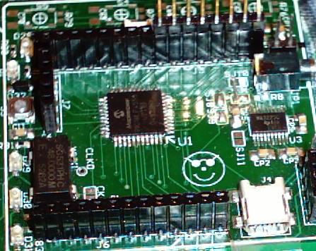
After boards with a smiley or two on them* failed to raise any eyebrows, my first big “art project” converted a monochrome bitmap and placed it on the silkscreen. Completely gratuitous and nonfunctional, but they didn’t whinge about it, so I assume silkscreen ink doesn’t really cost. The quality of the silkscreening on these boards wasn’t that great, though (possibly on purpose ;-) – it was smudgy and scratched/rubbed off easily. So the next superfluous board art was placed right on the copper layer, where they couldn’t crap it up. This required more care to avoid triggering design-rule violations, but also came back with no complaints. (This board also violates the “no multiple layouts” rule explained below; a small accelerometer board is laid out inside the unused space.) Between JR and myself a few other “I’d love to know what happens if…” shits-n-giggles suggestions were made, such as inverting the silkscreen layer so that the board is entirely coated in white, or adding text like “PCBFABEXPRESS can lick my hairy beanbag”, or covering every mm of the board with “active” circuitry (or a crosshatch pattern, etc.) so that there’s no place to stick the little logo they put on every board by default. We haven’t tried them (yet).
Holes per square inch
They’ll complain and charge extra if the board averages more than 25 holes / in^2. This actually does make some sense; the holes are drilled by machine, so more holes mean more wear & tear on the machine / drill bits. The cost for the boards themselves is based on a size range: e.g. there’s a fixed price for any layout 10in^2 and under, and another fixed price for anything between 10 and 20in^2, etc. When calculating “holes average”, though, it appears they base it on the actual board dimensions, not the size range your order falls into. In other words, the situation can easily arise where increasing the board dimension (e.g. leaving wasted space) reduces your cost for the order, even though this reduces the number of customers’ layouts they can fit onto the panel. (This did happen to me once; since I was running against a deadline I just let them charge rather than waste time trying to dick around with ’em. But I’m curious to see what happens if I say to just grow the board dimensions to reduce the average.)
Any attempt whatsoever to stick multiple circuits on one board
Is heavily frowned upon, although the reasoning doesn’t really make sense. The rationale is described here. They believe a panelized layout represents getting free stuff; I say it represents getting 10in^2 for the price of 10in^2. (Other than the “holes” issue described above, the manufacturing cost is a function of square inches, not what you do with them. Imagine if Kinko’s claimed you were getting an undeserved freebie and charged you extra for photocopying documents with small fonts…)
Long story short, we’ll agree to disagree. It can definitely be argued both ways – looking at the extremes, if I can just barely squeeze a 2nd circuit into the allocated space, they get a screwing since I don’t have to do 2 separate orders anymore; conversely, in the case of small boards, if I get charged for 10in^2 on my 1in^2 layout, I get a screwing as do the 9 other customers whose 1″ boards were made on “my” panel.
Rather than get into a long philosophical discussion / MATLAB plot of screwing ratio vs. board size, corner cases, etc. (is that one 8-channel filter or eight 1-channel filters?), let’s attempt to discover what they consider to be multiple projects.
Short answer: Pretty much anything can be argued as “same project” as long as there are at least two traces in/out of any area and all the part numbers are unique. The silk seems otherwise ignored (although I wouldn’t recommend placing a big dotted line and “cut here” scissors on it anywhere). This is only my own not-so-scientific (small sample size) observation; whether any given board is accepted probably depends mostly on who reviews it.
What’s worthy of note is that the design files are essentially raster graphics files; no text is stored in the files. This means no dupe-finding by script; a live human is paid to sit and scrutinize board layouts for these types of things. I kind of wonder whether or not they make out on separated orders vs. the overhead of the partnumber-checker guy and rejected/cancelled orders.
Board: WBSFMSv1r0 (before I started giving boards human-friendly names for reference) – strain gauge measurer and more
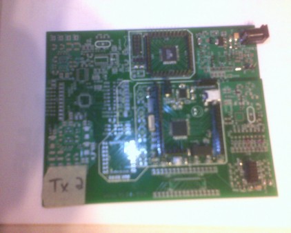
This one was manufactured with the $50 “too many holes” charge (hey, I was on a deadline), but without any complaint about separable sections. The board includes an FPGA evaluation unit and a small LCD “surfboard”; the rest is officially part of the same design, although the radio module (far right) and CPU / CPU+FLASH (center) can be cut loose along the white lines and used separately.
Board: Suncloud – LCD, tamper detection, and something else
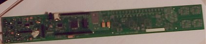

This board features an LCD driver board on one side, a big tamper detection dealie in the middle, and a tiny circuit tagged onto the far right side… quite obviously route-and-retain’ed, but no complaints here either. Sending it as a separate project, we would have paid at least $80 for 5 miniscule boards that may or may not have worked (it uses a part not solderable by mere mortals; we tried the ol’ heatgun-until-something-melts method with > 20% success rate); here we got 4*5=20 of them “for free” in the unused space of another layout. (This is why board houses should just charge by square inches + setup fee, not this cracked-out system of size ranges and extra charges and board scrutinizers.) Since the side circuit was so small and simple, we left their partnumbers off and replaced them with a single identifier per board. The boards are small enough they can easily pass as the footprint of a single part!
Board: Pandora – Battery-powered tamper detection and blinky lites
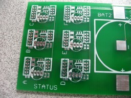
Same story – only 3 token traces connect these clearly route-and-retain blinkenlight boards to the main layout, an anti-tamper circuit for shipping boxes. AC says to me “…and it goes with this box, so we could call it Pandora, as in Pandora’s Box, heh, get it?” I’d just named it exactly that. Eerie.
Board: Switch – some little switching stuff, and an image sensor
I’ve been getting steadily lazier at drawing fake traces / etc., and basically just pasted a bunch of layouts together. I did run a batch-renumber script to uniquify the part numbers, but didn’t check its results very carefully – partnumbers of ICs were still duplicated. BZZT! They called me on this one, sticking their paw out for another $150 citing the dupe part numbers on the silkscreen. Oh Noes! Since this time I wasn’t in any hurry, I tried calling their bluff: I wrote back pointing out how much business we’ve thrown their way over the years, the fact that it costs no more to make a dupe-parts board, and that it would take me less time to just send it elsewhere for fabrication than renumber parts / add bogus traces and rebuild the design files. But they stuck to their guns. Enough of this BS; I told them to cancel the order and sent it to Gold Phoenix**.
Holes overlapping pads
One recent layout contained an unavoidable (due to size constraints) mounting hole overlapping a through-hole pad; within a few mils of the other hole itself. I thought for sure they would bitch about this, but they didn’t.
Silk covering pads / silk beyond edge of board dimension
It appears they postprocess the gerber files to remove silkscreening that overlaps a pad. I’ve also had silkscreen that extended about an inch beyond the board dimension (presumably, onto someone else’s layout) with no complaints, so I assume these are also removed during the process.
So there you have it folks – some initial research. There are some things yet to test! If anyone does (or already has), post a comment!
* a common practice (at least in our lab) is to place dummy “parts” on a schematic for components that don’t actually appear in the circuit, but still have to be ordered – like knobs or little sticky feet – so that they show up on the bill of materials. One or more guys were fond of naming the mounting holes with a partnumber for such parts, which occasionally meant adding extra holes when there were more extra parts than holes. But when one of my layouts called for 30 rotary switches(!) with knobs, rather than create swiss cheese, I created a part consisting of a goofy smiley face on the silkscreen. From what I understand, the meme is spreading (*cough* GJM *cough*) :-)
** who did it for much less, gave me more boards than I know what to do with (155in^2 for $119!), and even provided free step-and-repeat and v-scoring.
Leave a Reply