Goldmine Electronics LCD pinout (mini-teardown)

Goldmine Electronics has this funky unknown LCD (p/n G15623) available for 50 cents each, most likely surplus from a defunct cell phone production run. That’s wicked cheap for a good project LCD, since trying to snag most any decent graphic LCD is either impossible in small hobbyist quantity, or ridiculously expensive. A few affordable displays are available, but they tend to be these big ugly industrial affairs, often with suboptimal controllers, poor readability and lacking onboard RAM. If you want something smaller or looking less like Soviet-era castoffs for your project, you’re up a creek.

As with many surplus electronics items, these nice LCDs are offered cheap precisely because they come in in a huge brick of leftovers with no documentation; nobody has any info on the part’s specs or how to drive them. Semiconductors with no datasheets or even pinout information are 100% useless*. The LCDs come in a package of 2 for $1, so I bought a package and took it apart to see if I could figure out how to make it work. Hey, it’s more fun than Sudoku :P

Package & Dimensions

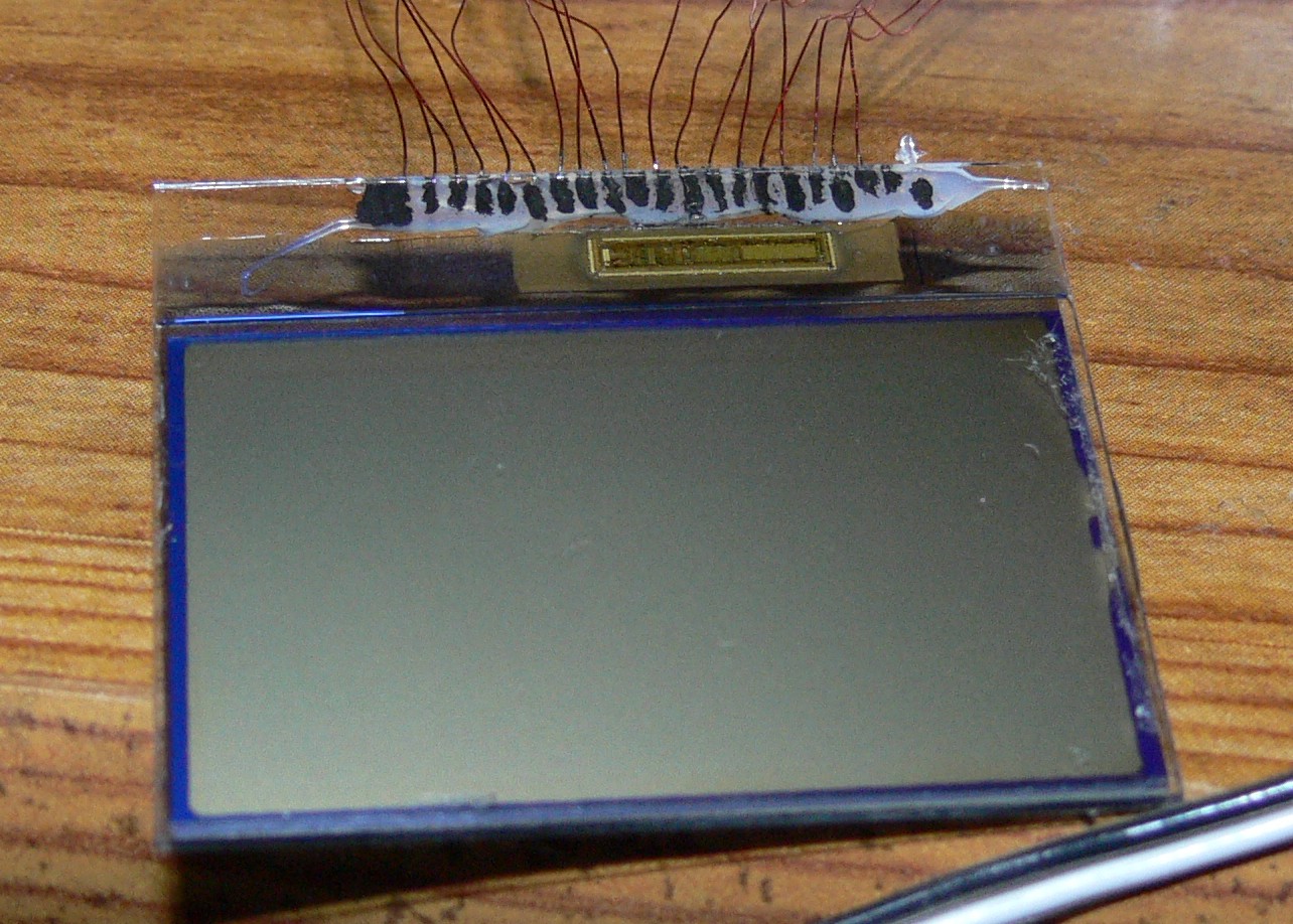
The display is about 1.4″ wide by 1″ tall, with some of the vertical dimension being for the elastomer (zebra strip) connection (most of the horizontal area is viewable). It features an integrated clear enclosure and backing (it appears to be made for easy LED backlighting) with a silver metallic rim. The metal/plastic enclosure bits are easily removable without harming the panel. There are a bunch of numbers on the back; one of these helpfully identifies the controller IC bonded to the glass (more on this below). This text reads:

79Z93 SDI 13-04 S6B0755
H2.80 REVERSE UG-09B63-AA B31

Zebra strips are a pain to work with for many hobby projects; it pretty much requires you to lay out a PCB, and work out the mounting of the display (with appropriate cuts for tabs, pegs etc. that you don’t have an Eagle footprint or drawing for) so that your board / enclosure / etc. firmly squishes the strip against the board. But if you’re willing to go this route, you have a small, cheap and easy-to-use display for your project.

Controller
The display features a chip-on-glass (COG) controller with onboard display RAM, which is a huge plus. (On RAM-less displays, much of your memory and CPU horsepower goes to sending the same image to the screen over and over at 60 times a second…with larger displays, your average microcontroller isn’t fast enough even to do this and nothing else.) Bits of black tape cover the controller IC and the glass on the opposite side of it.

The controller is a Samsung S6B0755, 128 SEG / 65 COM driver+controller for STN LCD (datasheet available at AllDatasheet). It includes the display RAM, on-chip oscillators for generating the LCD drive voltages, with full software control (no fiddling with pots or resistor dividers trying to produce a viewable contrast).

HOWTO: Get the pinout of a COG device

But how do we get the pinouts?

We’ve got the partnumber and datasheet of the controller, which is already more than I had hoped for. So what now? Well, from the datasheet we can work out some “required” traces, these would be the VDD/VSS, reset line, Cxx (the chip is far too small to have onboard 1uF+ capacitors!), CLK/DB6 and SID/DB7 ones. There are some other important ones, but many of these could be tied high/low on the glass itself depending on the configuration in use. The indicated pins have to come directly out. Peeling off the top tape gives us no new information; sure enough, there’s a little unmarked chip bonded to the glass. Peeling the bottom tape, however, gives us a clear (literally) window into the pin/bump configuration and registration marks (tiny symbols on the die to help an automated pick ‘n place machine align it precisely with the on-glass traces) as well as a rather breathtaking look at the die itself. If you haven’t noticed, this thing’s Frickin’ Small. I don’t have a microscope handy, but I do have a Kick Ass Digicam that can manual focus down to about an inch. There’s enough optical resolution that you can make out all 317 pads (inside a package of 9.5mm x 2mm!) fairly clearly. In the image below you can see the alignment marks, indicating pad 1 is on the bottom left (numbering will continue counterclockwise from there).

Up-close view of the COG controller and connection pads
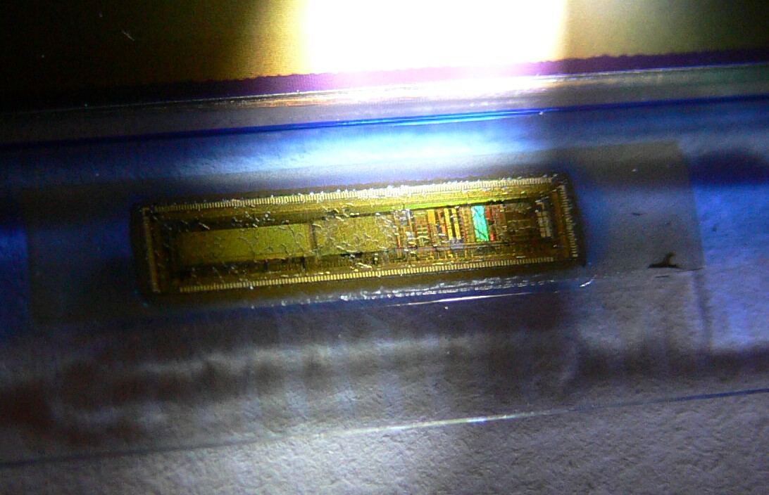
Up-close view of the controller die and connection pads. Click for larger version.

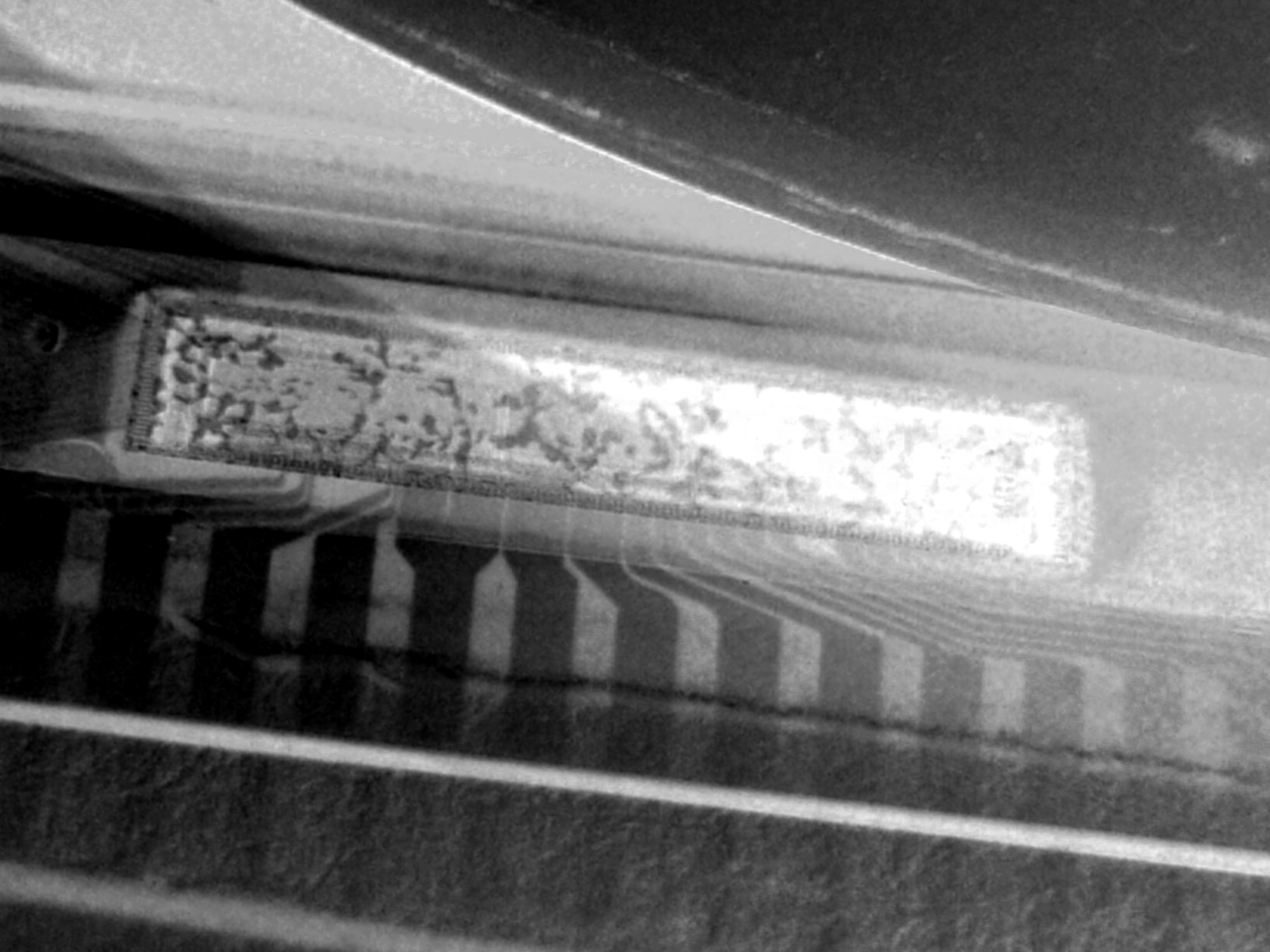
The connections on the glass are made by ITO (Indium-Tin Oxide) deposition. This conductive material is (by design!) almost completely transparent, but can be made to impart a bluish tint if light is bounced off it at just the right angle. Using a white LED keychain flashlight (also from Electronics Goldmine), the following picture and some others were taken with the ITO traces visible. (Best results were obtained by positioning the LED and camera so that the traces of interest were directly over the reflection of the glowing LED package.)

ITO traces on LCD glass

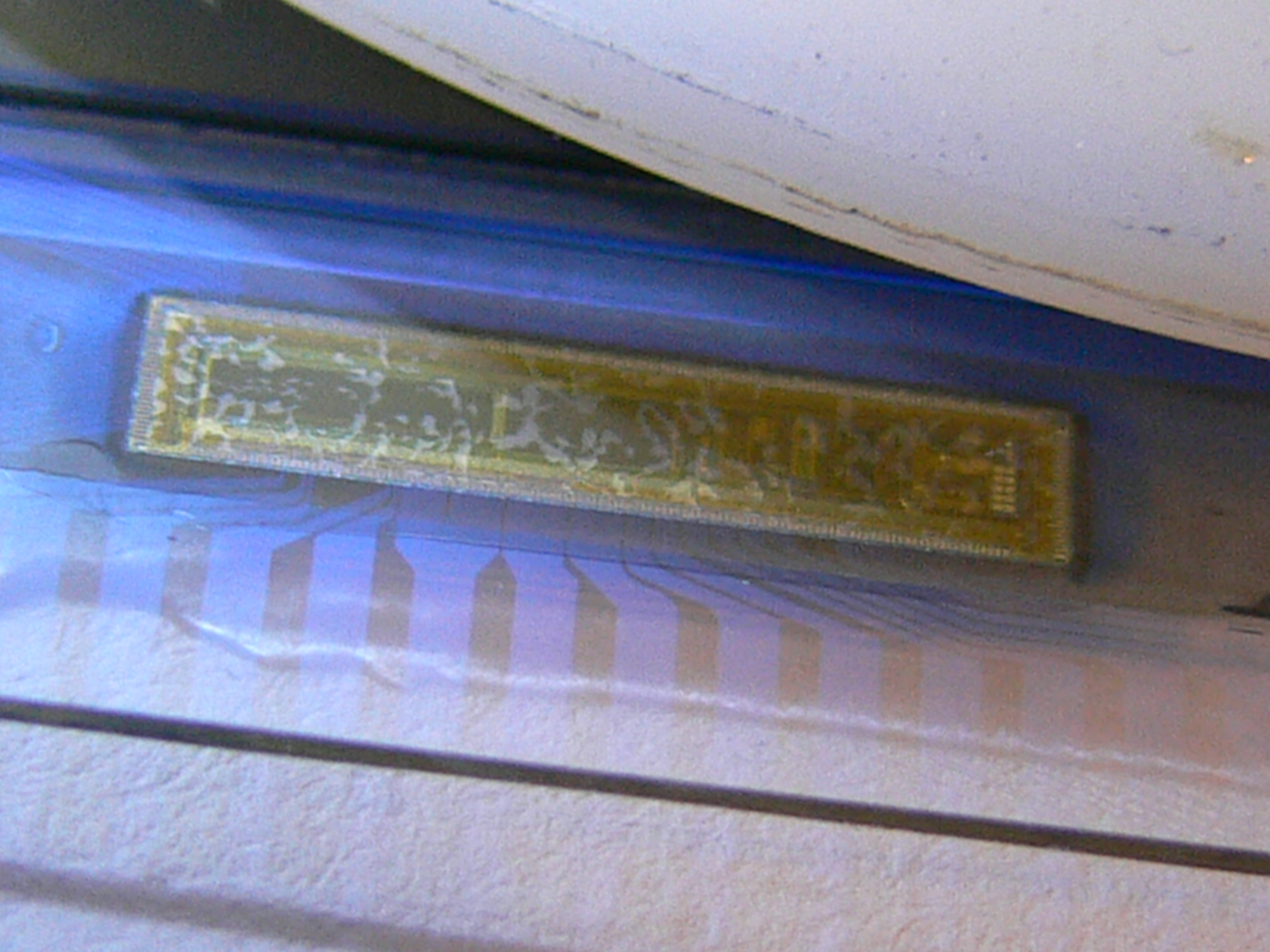
Image showing the important ITO traces and their approximate destinations. Click for larger version.

The traces are tough to make out, but since we know they show mostly in the blue-green portion of the spectrum, a little monkeying around in PSP (splitting the color data to CMYK, throwing away the unwanted channels and recombining) makes them show a bit more clearly (the traces appear here in black). It would have been nice to get a clear image of both the traces and pads at the same time, but no dice. This was proving next to impossible even with Kick Ass Camera (the angle required to show the ITO deposits prevents the entire thing from being in the focal plane at a time!) so our “required pins” (and inferences about how much juice they carry) will come in handy since trying to count pins would be a royal pain. We know VDD and VSS, the main power connections, are going to be side-by-side near the center (from the ‘Pad Center Coordinates’ table on page 5) and heftier than most. From the picture, we see three very fat traces going into the chip; the leftmost of these covers over a dozen pins, with a little bitty split in between. This must be VDD, which is also tied to VCI (Voltage Converter Input), hence the little split (which is not really necessary). Immediately to the left of these are two thin traces, these must be some small-signal data lines, Indeed, CLK and SID are right there in the table. Not surprisingly, a large gap between these and the next ‘required’ signals on the left (meaning the parallel data pins, and thus also RW_WR and E_RD, are not used). Working out the remaining connections is pretty straightforward.

Pinout

Pin numbering is relative to the ‘front’ of the display, with Pin 1 starting at the left. The first two don’t lead anywhere.


Pin / Name

1 NC
2 NC
3 CS1B
4 RESETB
5 RS
6 CLK (serial clock; parallel interface not supported)
7 SID (serial data input)
8 VCC
9 VSS/VSS2
10 VOUT
11 C3+
12 C1-
13 C1+
14 C2+
15 C2-
16 C4+
17 V4
18 V3
19 V2
20 V1
21 V0

Attachment, sans zebra strip

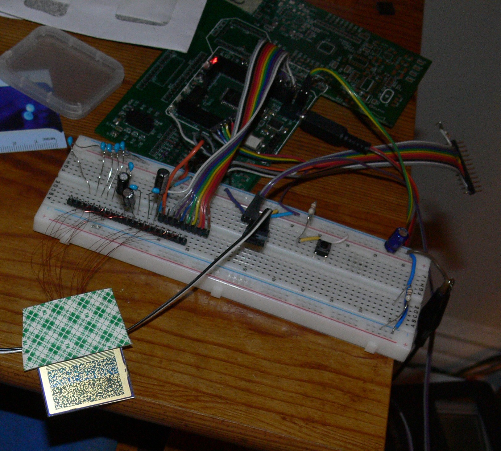
Ordinarily, to use the zebra strip you’d lay out a board with pads lining up exactly with the active bits of the LCD glass via the strip, and find some way of smashing the strip firmly against both the glass and the board. But I’m feeling ghetto and don’t want to spin a board just for this, so I’m trying an alternate approach. In my Goldmine order I also picked up a small bottle of “Amazing Wire Glue”, a relatively inexpensive conductive glue. (Usually such materials, e.g. silver conductive epoxy, are on the pricey side.) So here I have laid out pre-tinned strips of the smallest magnet wire I could find in the lab on a piece of thick double-sided tape so they couldn’t move around, and very carefully bonded them to the ITO traces. Since it would really suck to have one rip loose later, once the glue dried for a bit I gooped epoxy over them all.

Faking zebra strip connection using magnet wire and Amazing Wire Glue.

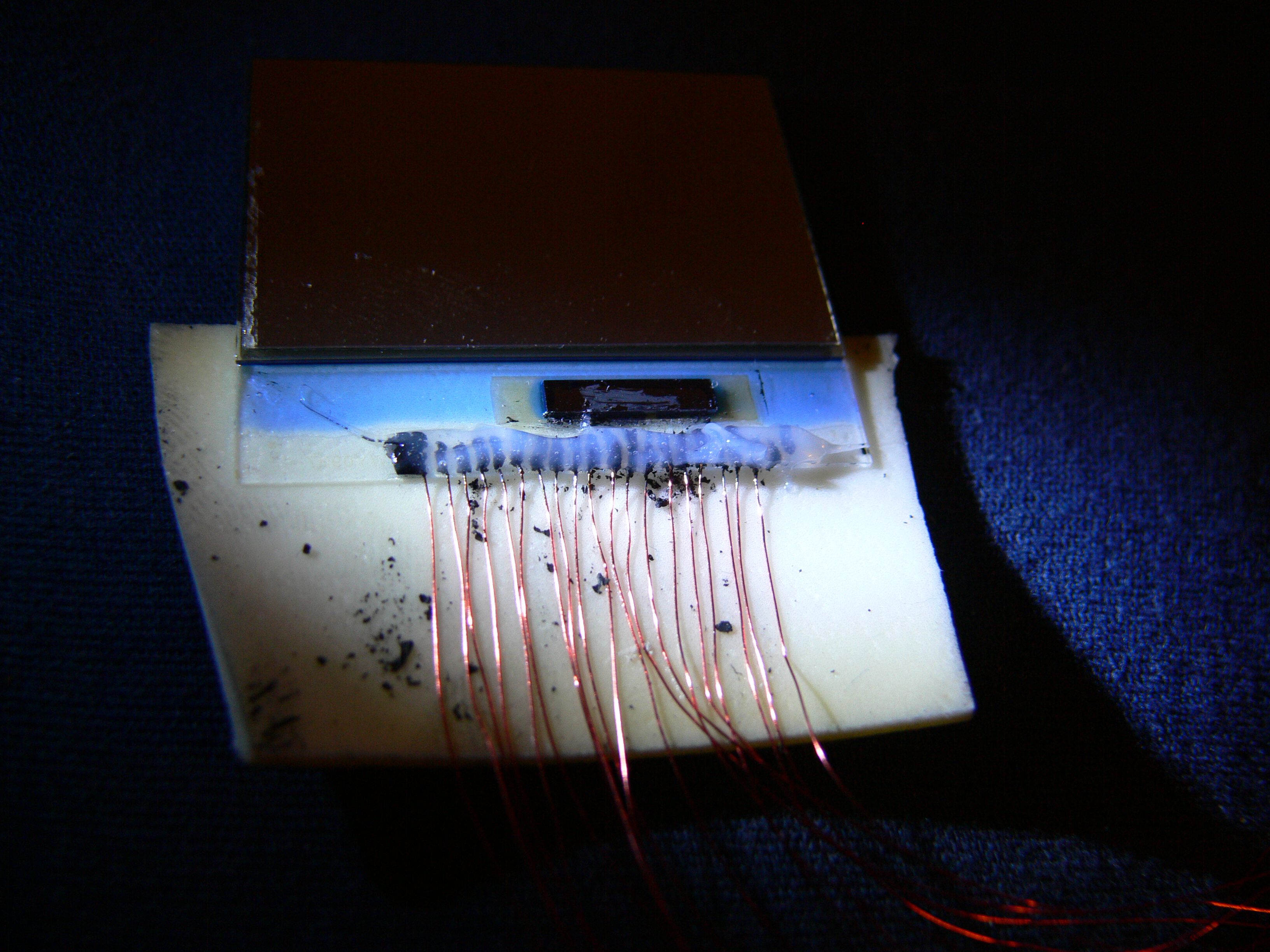
You can also see how the glue job looks from the front.

Fire it up

The controller datasheet gives the recommended circuit hook-up (capacitors, etc.)…I used a VCC of 3.0V since that’s the regulator I had laying around, and the “Triple Boosting” configuration. I couldn’t get the others to work reliably, most likely having something to do with the long wires between the switching converter pins (C1+, etc.) and capacitors…the resistance of the carbon glue (which I haven’t measured) may be a factor too. All in all this whole setup was pretty unreliable (e.g. fading in and out somewhat); hopefully a real PCB layout with the switching caps as close to the display pins as possible will work dependably.

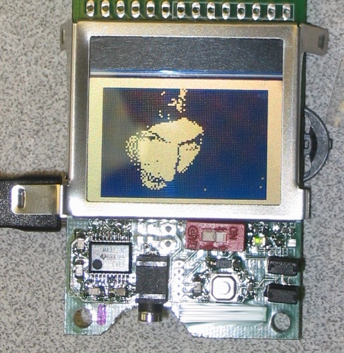
I loaded a variant of my standard LCD test image onto a spare PIC18 board. Here is also a picture of some random display memory contents on start-up.


Goldmine LCD displaying Evil Tim test image
Goldmine LCD displaying uninitialized memory contents

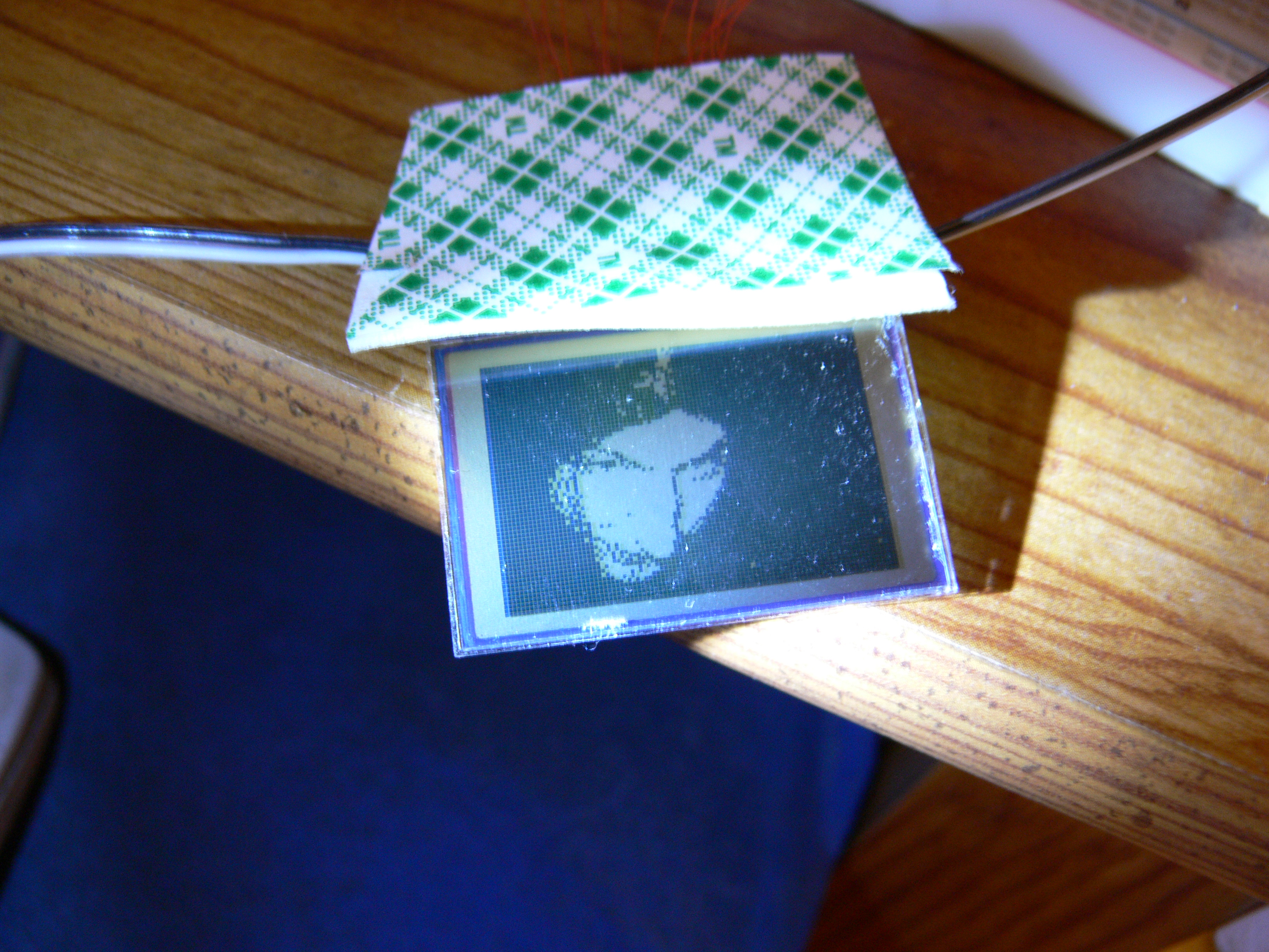
I say it looks pretty good in its reflective mode. The backing is actually “transflective”; sort of a one-way mirror that reflects ambient light well while allowing backlighting to also pass through. Lit from behind, it’s not quite so impressive.


Goldmine LCD with ghetto LED backlighting

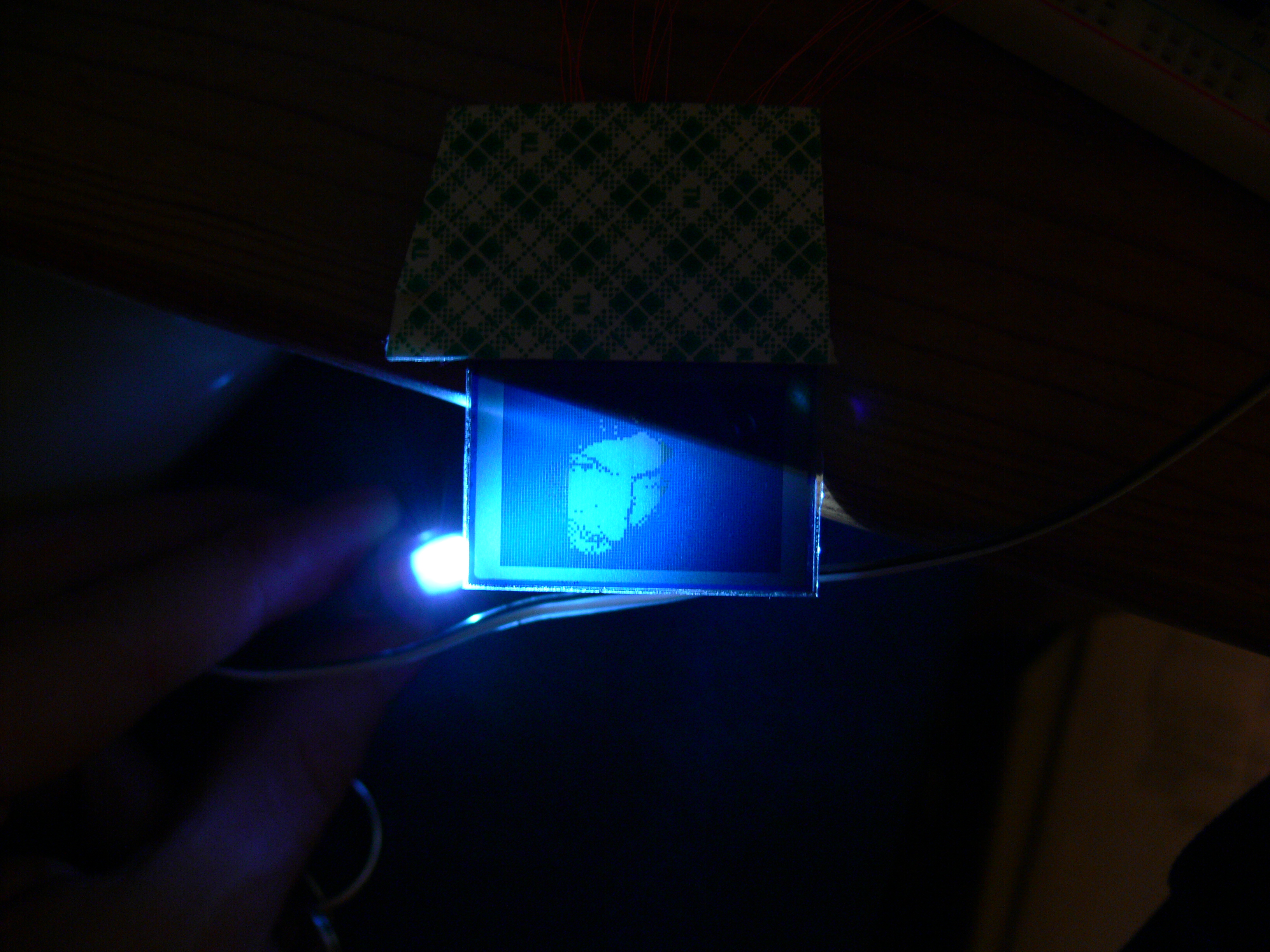
Note: Even though some of my pics show the die still exposed, don’t do this – the semiconductor junctions are sensitive to light, so exposure could cause undesired operation. Mine was going dead and resetting itself every time I took a flash picture at close range.

Setting up the controller registers correctly was a bit of an exercise. Some of these settings will depend on your rail voltage and which boosting configuration you use.

My settings are:

Name Value Notes
Set partial display duty ratio 010010xx 01000000 1/64 (highest / normal) – it’s a 64-line display
Power control 00101111 All power circuits on, use internal everything
Select DC-DC step-up 01100000 Triple boosting for me. Change as needed for correct LCD contrast based on your VDD voltage.
Select regulator resistor 00100111 Maximum Vo. This is sort of a coarse contrast control. Tweak as needed…
Set electronic volume register 10000001 00111111 Currently set to max, but this seemed to have no effect for my ghetto circuit. This “should be” a fine contrast control.
Select LCD bias 01010001 1/5 bias. There is a great tutorial here on what these numbers mean.

The only settings specific to this display are the duty ratio, power control, and LCD bias. Aside from those settings above, follow the datasheet’s flow diagrams for the order of setting up registers, turning on oscillators and starting the display.

Schematic, EAGLE footprint and sample code!

This file contains a schematic, EAGLE library, and sample code in C and PIC18 assembler: goldlcd.zip

Both show the basic code necessary to initialize the display and display an image. The C example includes a character generator and functions for text and bitmap display.

The schematic and footprint are verified as correct, as shown below :-) To allow the metal tabs on the LCD to clamp onto the circuit board, the board must be 0.031″ thick (e.g. half-thickness; if you don’t specify otherwise most board houses will give you 0.062″)

*okay, not entirely useless. In my lab we have a corkboard with a big bin of cheap opamps in a DIP8 package as thumbtacks.

Comments

37 responses to “Goldmine Electronics LCD pinout (mini-teardown)”

  1. Valery Avatar

    Wow, you’re cool, man! Here in Russia we have such devices of famous vendor “Noname” too :) Thanks for ideas.

  2. dk Avatar
    dk

    I just bought a couple of these, and was thinking, this on will be hard to figure out, but you did all the hard work. Great job! If I had bought these two weeks ago, I’d have been out of luck.

  3. bill Avatar
    bill

    Nice work. Did you get spacing of the on-glass contacts for creation of a hypothetical PCB? If the chip is 9.5mm, it looks like a bit less than 1mm from your photos; small but well within homebrew PCB range (though I guess there should be gold, too, which would be a bit tough…)

  4. Tim Avatar

    Hi Bill,
    I measured the pitch of the contacts at 1mm exact. The leftmost one is about 5mm from the left edge of the glass. I can’t speak for longterm reliability compared to gold, but for hobbyist purposes straight tin, or better yet silvered pads (some PCB houses, e.g. Gold Phoenix offer this as their “RoHS” option) should be fine. If you’re laying out a board for them, be sure to order a couple ahead of time an take apart one to get the measurements exact! The LCD has clips on the sides that can mount it securely to a board (no glue/etc. required) if it’s sized just right. I think the clips are made for a 1/2 thickness board (.031″).

  5. Jim Avatar

    bill, let us know, we are making pc-boards already…

  6. bill Avatar
    bill

    I’m not likely to have anything soon. I wonder if Goldmine has enough of these to make it worth the trouble; that’s one of the problems with surplus sources; they dry up :-(

  7. Sudoku Avatar

    if you are into Sudoku you shall check out Kakuro which is a new puzzle game that’s getting popular lately :-)

  8. Zach Avatar

    I just got 13 (!) of these things when I bought one of the super electronic surprise boxes. They also included an 8×24 lcd panel made by hyundai which seems to be well documented, which made up for the hundreds of 820 ohm resistors they included.

    Unfortunately I destroyed one before I saw this page. I still have 12 left, and absolutely no idea what I’m going to do with them now (other than hold on to them, now that I know I can actually use the things.)

    I suspect that they have a lot, and are trying to figure out how to get rid of them.

  9. Zach Avatar

    So, in furtherance of possibly doing something with the screens I have, I decided to build a breakout board. Unfortunately I didn’t get as much time this weekend to work on this as I would have liked, but I think I have something useful.

    By taking measurements and comparing against this info I have come up with a breakout board. It has spaces for the caps and the rest of the pins go to a 14 pin header. If I’ve set everything up right it should be perfect for using to experiment on these boards.

    If anyone wants to try etching this I’d be curious to see what your results are. I’ll be etching one for myself this next weekend. I’ve posted a PDF that’s (almost) suitable for transferring to a board. You’ll have to figure out your own way to flip the image horizontally. I do it at printing time normally, and for some reason I can’t get anything else to flip it without either shrinking or growing the image.

    If you do decide to try this board keep in mind I haven’t tested it yet. It seems to line up when I print it and hold it up to the screen, but there’s no guarantee it works.

    http://darkstar.frop.org/~zwhite/G15623%20LCD%20Screen%20Breakout%20Board.pdf

  10. ty Avatar
    ty

    these are displays from motorola v66 flipphones!!!
    i know this because i took apart my moms old cell phone.

  11. pethoviejo Avatar
    pethoviejo

    Ordered breakout boards from Gold Phoenix for this display. Etching the pads for the zebra connector was a bitch so I had it professionally done. They work great. Converted a ks0108 controller library for SPI using an ATMega128 and the STK500/501 dev boards and GNU-C. Nice little LCD for the price. Thanks Tim. Be happy to help anyone get started with this display.

  12. Jeff Avatar

    Tim – you are officially my hero… I just got one of these in a grab bag (having glossed over them individually, thinking they would be useless, like most cheap LCDs) and found your site as the first Google Result. (a miracle, considering how long it usually takes to find out *anything* about stuff like this)
    I’m in 1st year EE in British Columbia, Canada, but I have a decent amount of experience. My long-term project is to make a wireless-enabled wristwatch with this. (another miracle is finding a nice, easy-to-use LCD that my sister wouldn’t disown me for wearing on my wrist!)
    btw, if any other readers have bought a bunch of these, I could really use 1 or 2 more… I can’t afford to pay $18 shipping on a $2 order, and I really don’t care how long it takes to get here… jgm3 a|t sfu d|o|t ca – thanks

  13. Justin Avatar
    Justin

    I received a bunch of these in an electronic gold mine variety pack and was very interested in them, but the connectors put me off. Thank you for doing all this work! It’ll really come in handy!

  14. Frank Avatar
    Frank

    Would it be possible to see the code you (or someone else who got it to work) used to communicate with the LCD? I’m attempting to hack some together myself, but I’m running into problems initializing it.

  15. Tim Avatar
    Tim

    I just uploaded a zip file with some example code (C and assembler), schematic and an EAGLE library I made for the part – see the very bottom of the post (just before the comments start). Enjoy! It would be great to see what people manage to build with these displays.

  16. michael Avatar

    hey tim i got a few of these last time i orderd from goldmine in one of the boxes of random stuff.. i think i have 7 or 8 of them
    do you think they are worth the time or should i just leave them on the shelf??

  17. Frank Avatar
    Frank

    Hi Tim,

    Nice job!
    I really can’t figure out what is the need of J5 in the schematic?
    Can you please explain?
    Thanks

  18. Justin Avatar
    Justin

    Code and an Eagle part? Fantastic! You’re the best, Tim!

  19. Tim Avatar
    Tim

    Hi Frank,
    J5 is just there for debugging, you can stick a scope probe on them and verify that the voltage booster is running (voltages are flipping back and forth across the Cx+/Cx- caps). Otherwise this connector is not needed. All of the important signals are on J1.

  20. Tim Avatar
    Tim

    Also a general note, the capacitors (especially the Cx+/Cx- voltage boost caps) should be placed with short traces, as close to the zebra strip as possible! Long, high-resistance runs (like my ghetto glue-job above) will yield unreliable contrast / image quality. Surface-mount caps can be easily fitted underneath the display (see the PCB I finally made in the last image, the caps are lined up beneath the black tape on the display); through-hole caps could be placed on the reverse side of the board, underneath the display (the leads if properly clipped will fit easily behind the display), or on the front of the board just outside the area taken up by the display. (That is, if you consider the zebra strip to be the “top” of the display, the caps can be placed just above the display for close proximity to the zebra strip.)

  21. Frank Avatar
    Frank

    Thanks Tim for the J5 info!
    One thing also that is missing from this very helping post,
    is a picture of the back side of the LCD showing the zebra strip!
    It would be nice to see it…

    Regards,
    Frank

  22. Tim Avatar
    Tim

    Hi Frank,
    I can do this next time I am home. When I ordered my LCDs they all came with the zebra strip already attached – if yours didn’t, you might have just gotten unlucky, or it may have fallen off during shipping and gotten lost in the packaging somewhere. Check carefully around in the bag for a small flat rubbery thing!

  23. Frank Avatar
    Frank

    Hi Tim,

    Sorry I didn’t tell you that I haven’t received the LCD at the time
    I was asking for the zebra strip picture.
    But today I have received them! So there is no need for a picture…
    Thanks Tim for your help.

    Regards,
    Frank

  24. Tom Avatar
    Tom

    I found this display in a Motorola 120 cellphone. Thanks for the info!

  25. Frank Avatar
    Frank

    Hi Tim,

    I have seen your youtube video!
    Very nice job!
    I would like to ask if you have a PCB leftover,(the small one that has attached the LCD),I would like to have one, to run some tests.
    I can also send you a payment via Paypal if you wish.You can also email me to the email of this post.

    Regards,
    Frank

  26. Frank Avatar
    Frank

    Hi Tim,
    Any update for the above request?
    Frank

  27. dk Avatar
    dk

    Can you post a link to Tim’s video? I can’t seem to find it. Thanks

  28. michael axelrad Avatar
    michael axelrad

    Thanks Tim – awesome assistance – I am planning to use the display in a variety of sensor and control applications. See a working example here: http://picasaweb.google.com/lh/photo/lQVuC27WCtcGSbWVhkwIDg?authkey=xlVSGArs0ck

  29.  Avatar
    Anonymous

    Great stuff! Just got a bunch of these in one of Goldmine’s “surprise” packs- much more useful with this info!

  30. Eric Avatar
    Eric

    Tim – I built up a footprint for the gEDA/PCB tools based on the Eagle data you published. I’m planning a little board – details here: http://members.cox.net/ebrombaugh1/synth/dsPIC_lcd/index.html

    I noticed that there are recesses in the plastic housing which appear to be designed for backlight LEDs. Although it appears that they’re intended to be mounted on a small daughtercard that snapped into the back of the display, I’ve added silk indicators to the main footprint to align some 0805 pads. It’ll be interesting to see if this works.

    Eric

  31. Tim Avatar

    Eric,
    Sweet board! I’m interested to see what you do with it :-)

    I also noticed the cutouts in the LCD that seem to be for backlighting… my guess is they’re meant for those funky 45- or 90-degree surface-mount LEDs sometimes found in phones and gadgets (the DSLite uses them for LCD backlights), but I didn’t find any comparable part on Digikey. I tried some plain amber chip LEDs in those spots… they ‘worked’, but the light was somewhat concentrated near the bottom and not very bright. Really, I could only tell it was backlit at all in a dim room.

  32. Eric Avatar

    Well, I got the boards back from the fab and even though they are 0.062 the tabs still seem to grab OK. I’m running from 3.3V but still using the same configuration as your code. So far I’ve just tried the init sequence without sending any display data and I can see some difference in the waveforms on the capacitors. I’m not seeing anything near 10V though, so that’s a bit of a concern. The ‘all_black’ command doesn’t seem to do anything either – is this what you saw too?

    Anyway – I’ll keep poking at it but nothing conclusive yet, other than that the board seems to fit OK.

  33. Eric Avatar

    Hey – finally got around to fooling with my board again, prompted by some helpful hints from Kenny Booth. I’ve gotten one of the displays to power up to random bits, but others hooked to same board & same firmware just sit there (some even get kinda warm). No idea what’s up with that.

  34. Eric Avatar

    OK – got reliable operation of my boards with multiple displays. The trick for me was to clean _both_sides_ of the elastomer strip with IPA & cotton swab. After that 9 of 10 displays worked. One of the displays had an apparent scorch mark hidden on the glass side of the strip – that was probably the one that got warm.

    Anyway – success. Thanks.

  35. Sparr Avatar
    Sparr

    I got a dozen of these displays in Electronics Goldmine’s display assortment, and am very grateful that you did all the heavy lifting here!

  36. […] a common PCD8544-based display salvaged from an old Nokia cell phone. Since then, I got a small LCD breakout board from my fellow Dorkbot Boston member, Tim. The LCD itself is very similar to the one from the […]

  37. Ericfixit Avatar
    Ericfixit

    Thank you for doing all the work. Got some of these in a grab bag. First hot on google amazing
    Thank You… going to etch

Leave a Reply

Your email address will not be published. Required fields are marked *